One of the many challenges for the IC developers is to change the channel material to increase transistor mobility. But what about manufacturing? Can LED-style epitaxy be migrated to high-volume silicon manufacturing?
“The use of Ge and InGaAs quantum wells is an extension of the current strained Si strategy,” said Aaron Thean, vice president of process technologies and director of the logic devices R&D program at Imec. “The strain created by the lattice mismatch, and the confinement created by the interface between different materials, produce an improvement in mobility of around 2x.”
Thean’s group is working with a number of suppliers in both Si and LED supply chain to develop processes. “They are focused on epitaxy on the device wafers, rather than growing the materials separately and then bonding the pre-grown epi on the device wafer,” he said.
The bonding process is widely used in the LED industry to make thin LEDs, and was used for some early device experiments. Looking further ahead, Thean explained that they could build nanowires of silicon, with two dimensions of confinement. A multi-layer stack of Si and Ge layers is patterned and etched to form a nano-fin. The Ge is then removed to leave free-standing Si nanowires.
The Imec project uses direct epitaxy on 300mm device wafers. The research house is working with several established and new equipment suppliers. Thean pointed to some important differences between the quantum wells for channels—which were much simpler with only three or four layers—than those used for LEDs. He also observed that the successful introduction of Ge materials showed that the supply chain had learned how to manage the process cycle times.
Thean was emphatic that “it is all about defects.” What’s important here is which defects cause problems, and what are the strategies for managing them. One of the lessons from LEDs is that not all crystal defects are lethal, with GaN as the best and least understood example.
Imec is relying on their equipment suppliers to be ready for HVM, if and when the process and defect density issues are resolved.
Imec isn’t alone in its investigation of alternative channel materials. A number of equipment vendors are searching for new options, as well.
Although the channel structures published sometimes feature thin layers that appear similar to quantum wells used in the LEDs, they are driven by a different set of requirements,” said Swami Srinivasan, product marketing director for front-end products at Applied Materials. “The goal of new channel solutions is to place a material with as high intrinsic mobility as possible in contact with the gate. Scaling requirements in CMOS dictate dimensions that are small enough that quantum-confinement effects come into play, especially for some alternative-channel materials.”
Like Thean, Srinivasan believes that process defects are the big challenge with every new IC material. “In this case the problem is crystal defects caused by hetero-epitaxy that are extending into the channel. Dislocation defects could cause unwanted leakage, or impede carrier mobility, and thus lead to increased variability in device performance.”
He emphasized that this was a key research focus, and a best guess is that the acceptable defect density is lower than 1E5/cm². For comparison, the LED space uses much higher defectivities with nitrides grown on silicon sapphire for blue LEDs, but also much lower defectivities with arsenides/phosphides grown lattice-matched to GaAs for red/orange/yellow LEDs.
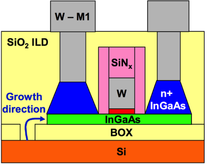
The growth process is the key to defects. One integration option is to employ subtractive processing, where a “blanket” layer is grown over the whole wafer and then etched away. Alternatively, additive processing just grows the channel where it is needed. When asked whether lateral growth techniques (used for GaN) could be applicable, both Thean and Srinivasan pointed to a recent IBM publication as a possible new approach.

Schematic of device built by IBM, using lateral overgrowth of InGaAs.
Over the summer, IBM announced a version of additive, in which the epi starts at a seed area, and then grows laterally leaving the defects behind. (“Confined Epitaxial Lateral Overgrowth (CELO): A Novel Concept for Scalable Integration of CMOS-compatible InGaAs-on-insulator MOSFETs on Large-Area Si Substrates,” presented at the June 2015 Symposia on VLSI Technology and Circuits, in Kyoto, Japan). This looks just like the lateral overgrowth approach being used to grow higher quality GaN for lasers.
Srinivasan emphasized that while there was plenty of learning from the LED world, the equipment has to be designed to meet completely different wafer size, throughput and defect density requirements. He declined to comment on throughput targets because that would depend on integration approach, device architecture and process utilized.
The concerns about throughput come from the experience of epitaxial growth in the LED world, where it takes 30 to 45 minutes to grow several microns of material. The thickness is driven by the need for a buffer layer to reduce defects, and thick p and n regions to provide sufficient lateral conductivity. In addition, there are multiple quantum well layers requiring multiple changes in gas mixture. In comparison, the fin height in an IC transistor is less than a micron, so even allowing for a seed region, the thickness will be a fraction of LED layer and only one layer counts. As a result, the growth cycle time should be significantly shorter than for LEDs.
The bottom line is that while defects are a primary barrier to new channel materials, the HVM supply chain is engaged.